Localization System
Introduction
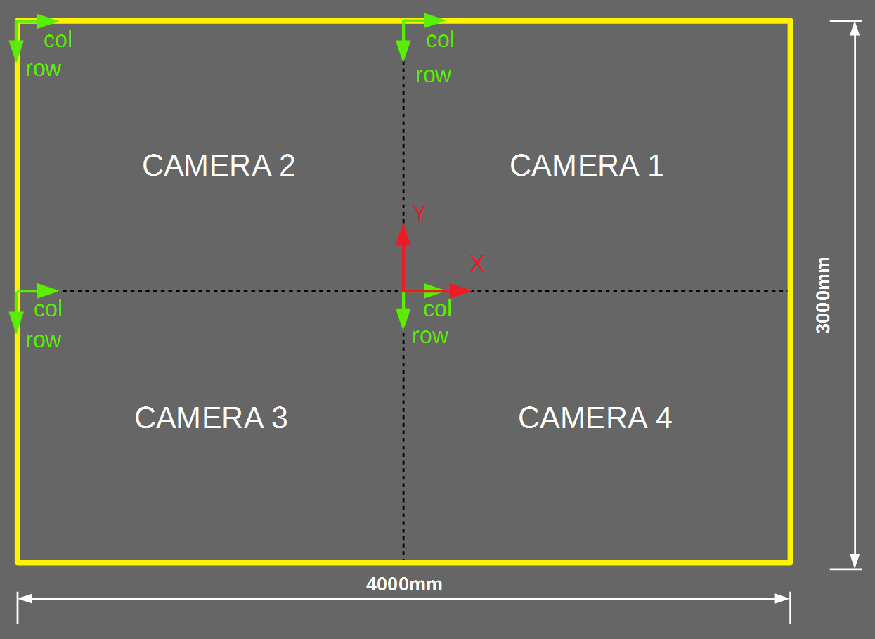
The UGV localization system used in UviSpace is composed by four camera-based localization nodes arranged in the ceiling in a 2x2 arrangement. The images from different cameras touch with each other without overlapping to maximize the field of view (and therefore the driving range of the UGVs). The purpose of having more than one localization node is just to create a field of view bigger than what could be obtained with a single camera. In total the cameras define an observable area of 3000x4000mm. The following figures represent the observable area (yellow), the camera numbering convention, the center of coordinates of UviSpace (in red) and the center of coordinates for the images of the cameras (in green).

FPSoC Localization Node
Each Localization node contains an FPSoC board and a CMOS camera. FPSoCs (Field Programmable System-on-Chip) are heterogeneous reconfigurable platforms consisting of a Hard Processing System (HPS) and an FPGA (Field Programmable Gate Array)in the same chip. The HPS is the non configurable part of the chip that contains a processor, cache memory, RAM memory controller, USB controller, Ethernet controller, timers, etc. This part of the chip is able to run an OS and programs like any of the common CPU-based boards: Raspberry Pi, BeagleBone, etc. In addition the FPGA brings the possibility to create custom digital blocks that help the processor in the execution, improving the overall performance. In UviSpace most of the image processing is implemented in the the FPGA while a small part of the image processing and the Ethernet communications are handled by the processor in the HPS. This scheme permits a higher frame rate (up to 100fps) than a processor doing all the work (around 15fps). The following figure shows a block diagram of the UviSpace localization node.
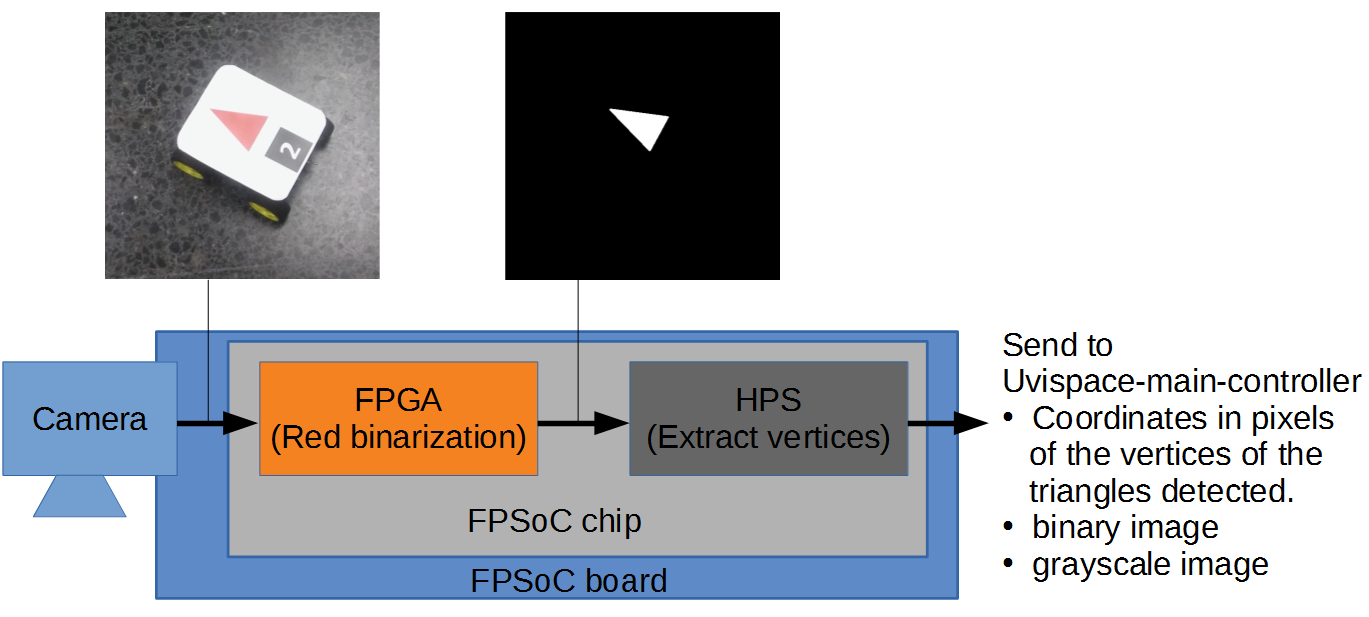
The localization node works as follows. The camera attached to the FPSoC board connects directly to the FPGA part of the chip. The FPGA captures images from the camera and does a preprocessing on them: each image is binarized leaving only red objects of the scene as white and the rest black. The UGVs carry a red geometric figure on the roof of the car so this is how its position is detected. The FPGA also generates a gray image from the RGB image, just used for visualization purposes. This part of the image processing is very time consuming on the processor, that is why it is implemented in the FPGA. After that, the images are saved into the processor memory and the HPS takes care of higher level tasks. The processor in the HPS reads the binary images andextracts the vertices of the red triangles drawn on the top plate of the UGVs. The HPS also implements a internet server and provides through ZMQ sockets the gray scale image of the scene, the binary image and the triangle vertices coordinates. The uvispace-main-controller connects to the server and asks only for the information needed. That means that the the information not needed by the main controller is not sent, saving internet bandwidth.
Note
The RGB image can be also obtained modifying the code of the server running in the HPS because extracting the RGB image and serving it reduced the frame rate considerably even when the main controller does not ask for it.
Hardware for the FPGA
In this section the hardware project to configure FPGA part of the Localization Node is explained. All code for the FPGA along with compilation and deployment instructions is available in the uvispace-camera-fpga repository.
Supported Boards
Currently the FPSoC chip used is an Intel FPGA Cyclone V SoC containing a Dual ARM Cortex-A9 processor in HPS and a Cyclone V FPGA.
The FPSoC boards supported are Terasic DE1-SoC and DE0-Nano-SoC. They are very similar to each other. Both have a Cyclone V SoC chip with exactly the same HPS containing a processor running at 925MHz and 1GB of external RAM. The FPGA structure in both boards is the same but they difer in size . DE1-SoC has a bigger FPGA (32070 ALMs and 496kB in memory blocks) than DE0-Nano-SoC (13460 ALMs and 164kB in memory blocks). Therefore more complex designs fit in DE1-SoC. Another difference is that the DE1-SoC has VGA connection while the DE0-Nano-SoC has not.
The camera connected to the FPGA is a Terasic 5 Mega Pixels D5M. It has a 40-pin connector.
The following picture shows a D5M camera connected to a DE1-SOC board showing the RGB image in a screen through the VGA connector. The seven-segment displays show the frame rate in the FPGA in hexadecimal (around 33fps).

The following picture shows a DE0-Nano-SoC board connected through internet. The gray image is received in a computer and streamed in a window using an utility in the uvispace-main-controller called get_video.py.

Recommended Tools
To program the FPGA we used the Quartus Prime Lite Edition 16.0.2 Build 222. We strongly recommend using this version to avoid generating errors when updating the project to a newer version.
General explanation
The following figure shows a complete diagram of the DE1-SoC version of the Uvispace camera. It includes most important elements of the Hard Processing System (HPS), the FPGA blocks and the elements in the board that are used in this application. We can divide the design in three main parts:
- HPS: The HPS is composed by a processor and useful peripherals like Ethernet and USB hardened in silicon. It can run independently of the FPGA running a full featured Operating System (OS) like GNU/Linux, Android or Windows embedded, so its like having an small computer in a single chip, like a Raspberry Pi or a BeagleBone. Its processor runs at 925MHz so software applications have great performance compared to the old way of implementing soft processors in the FPGA fabric. The HPS structure is fixed but some of its elements like HPS-FPGA bridges can be configured. This is done in Qsys (A tool inside Quartus that permits design of high level systems).
- FPGA Peripherals This part of the FPGA contains high level components that permit control of the Video Stream from the HPS. This components contain registers that are mapped into the address map of the HPS processor and connected to HPS-FPGA bridges using Avalon Memory Mapped buses. This part of the system is also configured using Qsys. Qsys permits in a single click the connection of standard complex buses like Avalon and AXI so it is very convenient for this purpose. The registers in these peripherals are connected to the lower level FPGA Video Stream control signals.
- FPGA Video Stream This part of the FPGA contains low level components that does not use stardard buses to connect components so all signals are manually connected and are configured using just Quartus (Qsys is not used). The blocks in the FPGA Video Stream contain the components to configure the camera, capture the video stream from camera, do the preprocessing (binarization) and send images to the VGA port. The basic connection between this blocks is a parallel bus with enough lines to transfer 1 pixel from one component to the next in a single clock cycle. It looks like a stream of pixels, like a river. So we can also call it video stream. Usually a signal travels with the pixels indicating in which clock cycles there valid pixels in the pixel paralle bus.
Lets now analyze every block in the 3 parts we just mentioned and do a little analysis of the clocks and resets in the system.

FPGA Video Stream Blocks:
Camera: The camera is connected to the FPGA using GPIO_1 connector in both boards, in the way it was shown in the pictures above.
Camera Config, available at uvispace-camera-fpga/ip/camera_controller/config_controller/, configures the camera every time it is reset. It sends commands through I2C that write into the camera registers that configures how the image captures and sends the image (image dimensions, pixel order when sending, exposure time of the sensor, etc.). Some parameters are made external and connected to the Avalon Camera component. This permits to modify these parameters from the processor.
Camera Capture, available at uvispace-camera-fpga/ip/camera_controller/, interfaces the camera and generates useful signals to control the image flow. The camera uses the following signals to sent the image: a 12-bit data bus (one pixel), frame_valid (1 when image is being transmitted and 0 during the vertical blanking), line_valid (1 during a line is being transmitted and 0 in horizontal blanking) and pixel_valid (1 when the pixel in the data bus is a valid pixel and must be used and 0 when the data bus does not contain a valid pixel so it must be discarded). Using this signals Camera Capture provides the 12-bit data-bus at its output and a pixel valid signal. To control where in the image the current pixel is it outputs X-Y coordinates of the current pixel and a frame/image counter. Switch 9 must be 0 in order this component to work, otherwise the video stream is stopped and you can see a frozen image when connecting a screen in the VGA.
Frame Sync, available at uvispace-camera-fpga/ip/camera_controller/frame_sync, is located between the Raw to RGB component and the Image Processing. It blocks the pixel_valid signal some frames. It is not clear in the camera documentation how the camera does the reset, if it does it instantaneously or if it first finishes the row that it is sending. This component solves this problem. Every time the camera is reset Frame sync counts few frame_valid negative flanks (end of the image) before letting pixel_valid propagate. This ensures that after this component, the 1st Raw to RGB sees after reset is the pixel 0,0. This is needed for some image processing components and the Avalon Image Writers to work properly.
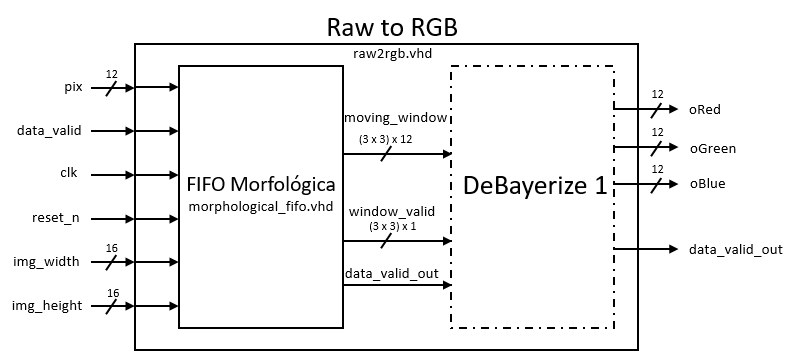
Raw to RGB, available at uvispace-camera-fpga/ip/camera_controller/raw2rgb, converts the raw pixels comming from the Camera Capture (each pixel in the camera contains only one color) to 3 component RGB pixels. The way to do so is using a DeBayerize 1 filter, based in a 3x3 window, as used in morphological operations (erosion/dilation) while using morphological_fifo.vhd. At its output it provides a pixel_valid signal that is 1 when a valid RGB pixel is at its output.
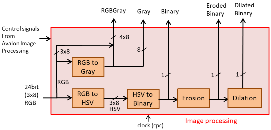
Image Processing, available at uvispace-camera-fpga/ip/image_processing, does the image processing computation needed in Uvispace. Each block inside image processing applies some operation to the pixels of the image, that are processed “on the flight”. That is, some delay can be applied to the pixels but the processing is different to software in which you store a full image and then process it. In hardware an incoming pixel is processed and put in the output as soon as possible. The blocks inside image processing use a pixel valid signal to tell to the next component that a new pixel has been generated. The image processing performs the following steps, depicted in the figure below:
- Transform 12-bit RGB to 8-bit RGB: the number of bits per component is reduced in the input of the image processing component from 12-bit to 8-bit. This is done to reduce size of image processing components and ease saving the pixels in memory because using 8-bit components each component ocuppies exactly 1 Byte (one address) in memory.
- RGB to Gray: each 8-bit RGB pixel is combined into a single component 8-bit Gray component. To do so the RGB intensities are averaged using Gray pixel = (2 x Green + Blue + Red)/4. Green is used twice because it is very easy to divide by 4 in hardware (2-bit shift) and difficult to divide by 3 and because it is more sensitive to human eye. Gray image is used only for sending to the uvispace-main-controller for visualization purposes. Pixel is delayed 0 clock cycles in this component.
- RGB to HSV: RGB is converted to the HSV color space because it eases the color binarization. In HSV Hue is color, S is Saturation (color intensity) and V is brightness (light intensity). This space makes easier to binarize a color just selecting a connected region in the Hue component. Pixel is delayed 6 clock cycles in this component.
- HSV to Bin: Using lower and upper thresholds for Hue, Saturation and Brightness the image is binarized. The output is a 1-bit component with 1 (White) for red objects and 0 (Black) for other color objects. We thought at the beginning that just using thresholds on Hue component were enough. But we later realized that very dark (black) or clear (white) portions of the image can be any color for Hue produccing noise. Thats why later thresholds for Saturation and Brightness were also applied. The binarization thresholds come from the Avalon Image Processing component and can be changed from the processor. Pixel is delayed 1 clock cycle in this component.
- Erosion: the morphological operation of erosion is applied to the binary image to remove small dots of noise from the image. The erosion kernel is a cross of 3x3. The output image gets delayed 1 line and 1 pixel and 1 clock cycle.
- Dilation: the morphological operation of dilation is applied to the eroded binary image to restore the original size of the geometrical shape on the cars roof (in example a triangle). The previously eroded noise does not appear again so together erosion and dilation make an efficient noise removal. The dilation kernel is a cross of 3x3 too. Therefore the output image also gets delayed 1 line and 1 pixel and 1 extra clock cycle with respect to its input.
Dual Clock SDRAM Controller, available at uvispace-camera-fpga/ip/sdram_control, stores the images for the VGA in an external SDRAM chip with 64MB of capacity. One of the images comming from Raw to RGB or Image Processing are writen into the SDRAM controller using the camera clock, used in most of the FPGA design, as we will see later. Then the VGA controller reads the images from the SDRAM controller at different clock. The SDRAM controller implements all the logic to access the memory from different clock regions without errors. This memory acts as a buffer between the image producer (camera) and image consumer (screen) so they can work at different frame rate.
VGA Image Multiplexers: A set of multiplexers are implemented to permit selection of the image sourced to the VGA controlled by:
- If Switch 5 is 1 the Dilated Binary Image is shown, else
- if Switch 4 is 1 the Eroded Binary image is shown, else
- if Switch 3 is 1 the Binary Image is show, else
- RGB image is show. Switches 0, 1 and 2 control the RGB individual components.
VGA Controller, available at uvispace-camera-fpga/ip/vga_controller, reads images from DUal Clock SDRAM Controller and converts it to VGA format. The VGA image is sent to an external chip in the board that sources the VGA connector (and VGA screen if connected).
Frame rate, a frame rate is calculated in frames per second (fps) in the top level component in hexadecimal and send to the seven-segment displays using 7-segment controllers available at uvispace-camera-fpga/ip/7-segment_displays.
FPGA Peripheral Blocks, implemented in Qsys:
PLL Camera Clocks: from the 50 MHz oscillator in the board generates a 24 MHz clock to source the camera.
PLL VGA Clocks: from the 50MHz oscillator in the board generates a 25 MHz and 191 MHz clock for the VGA.
Avalon Camera, available at uvispace-camera-fpga/ip/camera_controller/. It contains registers to controls the Camera Config parameters and provoke a software reset of the video stream (currently not working properly). Accessed by the processor through a 32-bit Avalon Memory Mapped bus. The available camera parameters that can be currently controlled by this component are:
- exposure: this parameter corresponds to a parameter called sutter width low in the camera that affects the exposure time (time sensor is open integrating light). It is not the only parameter that affects exposure but once all other parameters in the camera are set this parameter can be used to adjust the exposure time and adjust the brightness of the image. The more exposure time the more light is captured by each pixel resulting in brighter images.
- start_row and start_column: row and column of the first pixel of the image counting from the corner of the sensor. It permits to move the image window along the sensor area.
- row_size and column_size: defines the size (width and height respectively) in pixels of the image that will be sent by the camera in each frame.
- row_mode and column_mode: they specify skip (jumping rows/columns) and binning (combine few rows/columns into a single one). It permits to control the area of the sensor that we cover with our image resolution. We can do binning/skipping to have a small resolution image and still get a big field of view of the scene. Later we can remove binning/skiping and do a hardware zoom into some section of the image. The resolution is the same specified by row_size and column_size but the area covered is smaller than before.
- h_blanking and v_blanking: control the number “waiting” pixels after each row (horizontal blanking) and after every frame or image (vertical blanking). Most of parameters like image size, binning, color gain, etc. affect the frame rate of the camera. Using h_blanking and v_blanking, the frame rate can be controlled once the other parameters are set.
- red_gain, blue_gain, green1_gain and green2_gain: analog gain for each color component. The intensity for each color can me modified using this parameters.
Avalon Image Processing, available at uvispace-camera-fpga/ip/image_processing/. It registers to change the image processing parameters. Currently only upper and lower binarization thresholds for HSV components are available. Accessed by the processor through a 32-bit Avalon Memory MApped bus.
Avalon Image Writer, available at uvispace-camera-fpga/ip/avalon_image_writer/. This components saves images from the video stream into the HPS RAM memory so the processor can keep processing the images to extract triangle vertices or sending the images through internet. This components joins the 2 worlds, hardware and software. Since its little complex there is a single section for it in this page. Basically it goes always counting pixels from the video stream. Eventually the processor configures it and starts a new capture of images in a synchronized way. One special feature of this device is that it can pack several pixels and write them into the processor memory in a single bus operation, reducing traffic in the SDRAM Controller. There are 3 of these writers:
- RGBGray: Writes the 3 8-bit RGB components. Since the Avalon Image Writer can only have power of two inputs the gray image is added to the RGB lines to form a 4 x 8-bit = 32 bit input. The avalon data bus that writes images into memory is 128-bit wide. Therefore this component can pack 128/32 = 4 pixels and write 4 RGBGray pixels in a single bus write. The master bus of this component is connected to the FPGA-to-SDRAM Controller por 1 configured as Avalon 128-bit (so they fit perfectly). These ports are configured in the Qsys component representing the HPS.
- Gray: Writes the 8-bit Gray component. In this case 8-bit is a power of 2 so no dummy data must be added to the gray pixels to write them in memory. The avalon data bus that writes images into memory is also 128-bit wide. Therefore this component can pack 128/8 = 16 pixels and write 8 Gray pixels in a single bus write. The master bus of this component is connected to the FPGA-to-SDRAM Controller por 0 configured as Avalon 128-bit (so they fit perfectly).
- Binary: Writes a 8-bit version of the dilated binary image (last step of the image processing). Binary image is 1-bit per pixel. In order for the processor to more easily access pixels (memory addresses are per Byte, not per bit) 1-bit binary is transformed to 8-bit binary where all 8-bits are either all 1 or all 0. This 8-bit image is packed in the same way as the Gray image. Every 16 pixels a single write in the 128-bit bus stores them into processor RAM memory. In this case the master bus is also Avalon 128-bit but since no more 128-bit bus can be configured in the SDRAM controller we decided to use the FPGA-to-HPS bridge configured as AXI 128-bit (Avalon is not an option in this case). Qsys automatically transforms Avalon to AXI for us.
HPS blocks:
Microprocessor unit (MPU): includes two ARM Cortex-A9 32-bit processors, with 32kB L1 data cache and 32kB L1 instruction cache each and 512kB L2 shared instruction and data cache. A Snoop Control Unit (SCU) ensures coherency among L1 caches, L2 cache, and SDRAM contents.
Booting ROM: When the processor starts it first executes the code written in this memory, that basically does a basic configuration of some HPS systems (like UART to print text in console) and checks the MSEL pins to know were the next piece of code in the booting process is stored and copies it to the 64kB On-Chip RAM. In case of Uvispace next code is in SD-Card and it is called Preloader.
64kB on-chip RAM (HPS-OCR): it is used during start-up to run the Preloader. The preloader basically configures and calibrates the external SDRAM memory and loads the next code in the booting process in external SDRAM. That is called U-boot and is located in SD card in Uvispace (U-boot later starts-up all the HPS, configures the FPGA from SD-card, copies the kernel of the OS in RAM and launches execution to it. Learn more on Cyclone V SoC Booting Process here)). After start-up HPS-OCR remains unused and can be used as intermediate memory between processor and FPGA because both have access to it.
SDRAM controller (SDRAMC): It controls the access to the 1GB DDR3 external memory. It has a lot of ports that can do write or read operations on the external SDRAM simultaneously. These ports are: L2 cache controller (AXI 64-bit), L3 port (AXI 64-bit) and ports comming from FPGA (depending on configuration 6 to 2 ports, AXI or Avalon, 32, 63, 128 or 256-bit).
DMA controller (DMAC): Performs Direct Memory Access (DMA). It has a slave port connected to L3 that MPU uses to configure it and a master port connected to L3 too that DMA uses to copy data from one part of the system to other (including FPGA, ACP or SDRAM through L3 port).
L3 Main Switch: is a partially connected crossbar switch interconnecting all elements in the HPS. It connects masters accessing L3 (L2 cache controller, DMAC, FPGA-HPS Bridge and HPS peripherals with DMA capabilities) to the slaver (ACP, SDRAMC, HPS-FPGA Bridges). The Accelerator Coherency Port (ACP) allows perform coherent requests to the cache memories. All interconnection elements in HPS are AXI3-compliant.
Interconnection resources between the HPS and the FPGA fabric:
Those through which HPS accesses FPGA as master:
- The HPS-to-FPGA (HF) bridge, a high-performance bus whose data width is configurable as 32-, 64- or 128-bit (referred to as HF32, HF64 and HF128, respectively, in the remainder of this README).
- The Lightweight (LW) HPS-to-FPGA bridge, a 32-bit bus connected to the L3 Slave Peripheral Switch (referred to as LW32 in the remainder of the paper). Its performance is lower than that of the previous bridge. It is aimed at accessing the configuration registers of peripherals implemented in the FPGA fabric.
Those through which FPGA accesses HPS as master:
- The FPGA-to-HPS (FH) bridge, a high-performance bus enabling FPGA masters to access HPS peripherals, DMAC, and SDRAMC, as well as cache memories through ACP (coherent access).
- FPGA SDRAM configurable master ports, which access the external SDRAM memory in a non-coherent way directly through SDRAMC.
Clocks There are the following clocks in the design:
- CLOCK_50: 50MHz comming from external oscillator in the board. It is the base for all the other clocks in FPGA.
- clk_24: 24MHz clock generated in a PLL in Qsys System. It sources the camera.
- ccd_pixel_clk(cpc): 96MHz clock. Using clk_24 the camera generates the 96MHz clock. It is the clock used by the camera to transmit pixels from camera to FPGA. This clock is used in all the FPGA except for the VGA.
- clk_25: 25.175 MHz clock generated in a PLL in Qsys System. It is the base clock for a VGA of 640x480. Currently Uvispace only supports this resolution so it is the clock sourcing the VGA controller.
- clk_191: 191MHz clock generated in a PLL in Qsys System. It is the base clock for a VGA in HD. It is not currently used in the Uvispace.
Resets. The design has the following reset sources all of them negated reset (they reset when 0):
- HPS_RST Button: It resets the HPS in the same way as if power is disconnected and connected again. The HPS runs Preloader, U-boot, Loads the FPGA from SD-Card and finally runs OS.
- reset_stream_key: its a key to just reset the FPGA Video Stream (the part of the FPGA outside Qsys). This reset works properly. It is connected to KEY0 in both DE1-SOC and DE0-Nano-SoC.
- camera_soft_reset_n: it is a software source of reset coming from a register in the Avalon Camera component. It also just resets the video stream (the part of the FPGA outside Qsys). It is used by the uvispace-camera-hps/test_programs/camera_vga_test. This program changes the configuration registers in Avalon Camera and the uses the softreset to apply the new configuration. However it does not work properly. We do not know why. It is probably due to using normal lines to do the reset instead of dedicated reset lines. Because it looks like the reset is works slow and applies reset in different clock cycles. The FPGA works but the image in VGA has colors blurred/mixed.
- hps2fpga_reset_n: It comes from HPS and resets all, the FPGA Video Stream (the part of the FPGA outside Qsys) and the FPGA Peripherals (the part of the FPGA inside Qsys). This is applied by the HPS during start-up. It could be also used by software in the HPS but this was not tested yet. It works properly.
Summarizing resets. We have 2 resets with many sources. One that resets only the FPGA Video Stream part and other that resets all. Resetting all FPGA is only useful in start-up. Resetting the video stream is useful to apply a new configuration to the camera during debugging stages. During start up hps2fpga_reset_n resets all FPGA after configuring it. When reset, Avalon Camera default values for the registers are the correct for Uvispace. Therefore the camera is configured in start-up with the correct values and no more reset (using softreset or key) must be applied. Only when the parameters configuration of the camera are to be changed a software reset must be applied.
This explanation is valid for the DE1-SoC. The DE0-Nano-SoC project is exactly the same without the VGA related functionality (Dual Port SDRAM Controller, VGA Controller and Multiplexers) and the 7-segment.
FPGA Video Stream Details
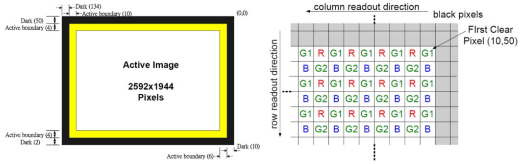
The TRDB-D5M camera captures a pixel array of 2752 columns and 2004 rows, but the active region consists of 2592 rcolumns and 1944 rows, because in the image borders a correct acquisition can not be ensured. The position row:0 and column:0 of the camera’s image is placed at the right upper corner. Image both areas can be observed in the following image.
The image brought by the camera controller is a Bayern Pattern image, exactly as it is captured by the sensors array. The Bayern Pattern consists of three color pixels, disposed as in the following image. The sensor brings a pixel stream at one pixel per clock rise edge, traversing the image by rows. Each pixel is encoded in 12-bit.
The camera controller returns 4 signals:
- PIXCLK: clock signal of 96MHz.
- FRAME_VALID: 1 when is sending an image. 0 since it finishes one image until it starts to send the following one.
- LINE_VALID: 1 when is sending a row. 0 since it finishes one row until it starts to send the following one.
- D: 12-bit bus with the pixel intensity value.
The following image shows the pixel regions that the sensor returns, and the values of the sensor output signals in each case.

The camera configuration parameters are:
- Start pixel of the image. Using start_row and start_col (Figure 11) you can move the start pixel of the captured image. This functionality, playing correctly with the other parameters of skipping and binning, allows the zoom hardware, without losing resolution.
- Size of the image captured by the sensor. Number of pixels per row and rows from start_col and start_row captured by the sensor. Use the row_size and column_size registers. Of the captured pixels not all have to be sent. The resolution of the image sent will depend on the configuration of skipping.
- Exposure. Increasing it results in brighter images with more vivid colors but decreases frame rate. Two values have been tested: the default one and the minimum for binarization to work correctly (for lower exposure values noise is so significant that it cannot be totally removed by erosion with 3x3 pixel windows, resulting in fake shapes being incorrectly detected or triangles being lost during some frames).
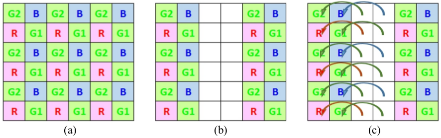
- Skipping. Reduces resolution while keeping the viewing area. Skip 1 and skip 3 have been tested, producing 1280x960 and 640x480 images respectively. In the following image, in section (b) a 1 column skipping of the input showed in section (a) can be observed.
- Binning. It can be used in conjunction with skipping to combine pixels from skipped rows and columns. This results in an image with reduced subsampling artifacts and softer borders, but also in a reduction of frame rate. Binning modes 0, 1 and 3 have been tested. In the following image, on section (c) a 1 column binning of the input showed on section (a) can be observed.
- Color Gains. It allows to modify the intensity of each color (applying a gain) in the image independently for each color component.
- Blanking. Clock cycles of the camera controller, after each row (Horizontal Blanking) and after each image (Vertical Blanking). It allows controlling the frame rate (reducing it), adding more waiting time to the minimum waiting time, already established by the sensor itself once other parameters are configured that affect the capture speed: image size, binning, color gain, etc. .
- Image turning. As a general rule, image sensors, when using a lens, invert the image in both axes of the plane. This sensor allows to choose the reading order of the array of pixels in both axes to undo the inversion of the lens.
Project Repository
All the HDL code involved in the Uvispace FPSoC camera is contained in three UviSpace repository main folders:
- de0-nano-soc: contains all the Platform Designer System code in order to implant de HDL in the board of the same name.
- de1-soc: contains all the Platform Designer System code in order to implant de HDL in the board of the same name.
- ip: contains all the low level hardware block implemented in the FPGA.
All the project repository folders contain a readme (.rst) file that explains the organization and function of the different files within it.
Platform Designer System
(Roberto) In the following picture we can observe the Qsys system just described as it looks in the program (some components were minimized cause they dont fit in a single Figure)
Present Qsys. Explain the picture. HPS block and the rest of FPGA peripherals. Export signals.

Qsys comment on _hw files. Each FPGA peripheral has a _hw file that creates a Qsys-compatible component from vhdl files.
Comment address map and show address map table with relative plus absolute addresses.
FPGA Resources Usage
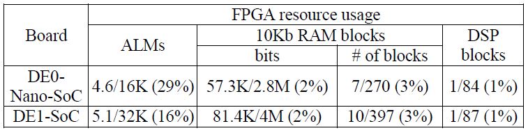
The system has bee tested in both supported boards (DE1-SoC & DE0-Nano-SoC). The FPGA resources usage is summarized in the table bellow. It can be noticed that, although being using low cost boards, most FPGA are still available for future extensions or updates of the system.
Work for the Future
(Delete this section because everything is done now)
- To reduce size of FPGA design using 10Kbit memory blocks to implement the morphological_fifo component. Now it is using ALM´s registers to store the lines needed to do a morphological operation.
- Increase the frame rate. It can be done changing the way images are captured and the Raw to RGB component. Instead of Using
- Fix the software reset that is not working. Maybe using the HPS-to-FPGA reset that seems to work.
- Reset the counters in Avalon Image Writers so it keeps synchronized when reset stream is produced.
Software for the HPS
General explanation
How the system works. It has LKM that does…. and application in Python…. Copy the paper explanation?
There are other applications, not used in normal operation, that permit useful tasks when debuging, like changing camera settings, image processing thresholds, etc.
Project Repository
Common files
Kernel modules: To learn more about kernel modules go to examples and install SD card Then explain one by one
Applications:
Precision and frame rate tests
Camera Setup
During the tests the following parameters have been analyzed:
- Exposure
- Skipping
- Binning
Precision in position estimation
The following table shows localization accuracy results. For each combination of camera settings and UGV location and orientation the standard deviation of 5000 measurements is shown.
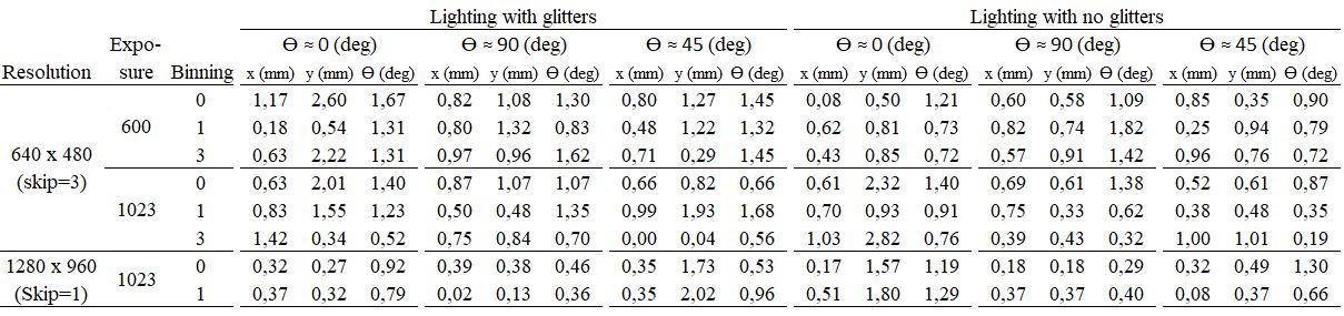
Regarding position, the worst result of all tested config urations is 2.82mm, but most values are around 1mm. The worst result for orienta tion is 1.82°. From a more detailed analysis it can be concluded that:
- Localization in the Y axis is less accurate than in the X axis.
- Orientation error and position error in the X axis do not vary significantly for the different actual orientations tested, but position error in the Y axis is noticeably affected. The worst result in the Y axis is obtained for 0º, and then for 45º.
- Localization accuracy slightly decreases when UGVs are located in brighter areas. This is mainly due to light blinking, which is more significant in bright areas than in dark ones.
- Using higher resolution (decreasing the skipping value) provides a mean error of 0.29mm for X, 0.80mm for Y, and 0.76° for θ versus 0.68mm for X, 1.02mm for Y and 1.05° for θ when using lower resolution. In other words, the improvement in accuracy provided by increased resolution is less than linear.
- Low exposure permits triangle binarization without negatively affecting accuracy.
Frame rate
Frame rate results are shown in the following table.
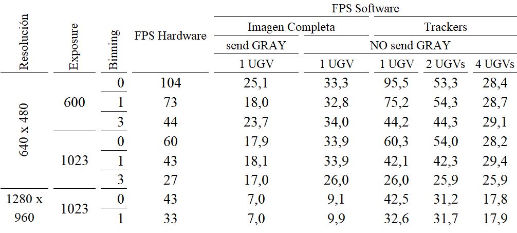
Frame rate results are shown in Table III. The hardware reaches a maximum of 104fps for 640x480 resolution and 43fps for 1280x960 when binning is 0. Higher binning values provide worse frame rates and, as previously analyzed, not better accuracy. Therefore binning should not be used.
When analyzing whole images the software frame rate is able to keep up with the hardware frame rate up to 33.3fps for 640x480 and up to 9.1fps for 1280x960. Regarding software trackers, they allow software frame rate to be increased up to almost hardware frame rate. 97.5fps (versus 104 in hardware) are achieved for 640x480 and 42.5fps (versus 43) for 1280x960. The performance of software trackers is very dependent on the number of UGVs in the image. Significant reductions can be noticed as additional UGVs are included.
When gray-scale or RGB images are simultaneously written along with the binary image from FPGA to processor´s memory and then sent via Ethernet, frame rate is reduced around 20%.
The best configuration can be selected by defining an adequate tradeoff between accuracy and frame rate. Increasing resolution allows accuracy to be improved up to 30%. Binning worsens both accuracy and frame rate. Low exposure offers similar results to those with high exposure for triangle localization. Therefore low resolution (640x480), low exposure (600) and low binning (0) is the configuration providing the best results: around 1mm accuracy at 104fps in hardware.
Installation of the cameras
Camera Set-up
Parameters selected, frame rate and size of the images for Uvigo Uvispace lab.
SD-card
(Roberto) Generate SD-card partitiopns and kernel get_current_corners_of_tracker Files to copy to the root folders Add file to configure ETHERNET and board connects internet alone Add file that automatically inserts driver and runs server
Make OS to load the uvispace-camera-driver on start-up. * Copy the uvispace-camera-driver.ko into the / * Create a .conf file wit <module-name>.conf insode /etc/module-load.conf. The modules in this folder will be loaded during OS start-up.
Launch the triangle-detector-server.py application on start-up. This is done using systemd utility that comes in the Linux kernel 4.
MSEL Switch configuration
(Roberto)
Physical placement
(Future) Modificaciones a la cámara Explicar las estrías del metraquilato para ajustar Hacer streaming y enrasar con marcas Ajustar con estrías
Cable connection
(Roberto) Power go to main switch in laboratory Ethernet to router, explain how router is mounted
Focus
Focus the camera using the wheel in the lens (put picture)
————-this was on introduction, integrate it here ——————- Physical layout ^^^^^^^^^^^^^^^
The main component of the vision system is a Terasic DE2-115 board, which contains an Altera Cyclone IV FPGA. With 115k logic elements, this is a fairly big FPGA, suitable for complex digital projects. Connected to the main board, through the 40-pin GPIO , there is a Terasic D5M 5 Megapixel camera.
In this project the 40-pin straight female header in the camera is changed by a 90 degree 40-pin header so the camera points down. 4 of these cameras are located in the ceiling of the laboratory like the following figure shows. The cameras are located so the field of view of the cameras touch with each other without overlapping. This is done this way to maximize the area the cameras can see. Problems to locate the car in the borders of the cameras should be solved by software.

FPGA hardware
The biggest part of the system implemented in this project is a NiosII processor system defined in SOPC-Builder. The rest of the system is defined directly in Quartus II.
FPGA software project
The software project that runs in the Nios II processor is basically composed by two subprojects:
- SocketServer, which is an application project containing the application-specific code.
- Socket_Server_bsp, which contains all the code that defines the interface with the hardware, creating an abstraction layer which eases the understanding, development and migration of code by a user.
————-this was on introduction, integrate it here ——————-
Uvispace IP Cores Documentation
In this section we perform a detailed description of some modules developed for the Uvispace project that are difficult to understand reading the code and are too complex to explain them in Hardware for FPGA section.
Morphological FIFO
Morphological FIFO is a subcomponent used in morphological operations (erosion/ dilation) and in the raw to RGB transformation. From the FPGA video stream pixels it returns at each moment the 3x3 window in order to apply the desired operation and a data_valid_out signal. It has to manage pixels that take part in the output window and the pixels that did not take part at all the output window positions yet (pixels at waiting positions).
For a 3x3 kernel, as used in Uvispace, it is based in a FIFO memory divided in five regions (shown in the image bellow):
- FIFO memory of 3 registers, which correspond to the three pixels of the lower row of the kernel at each instant.
- Wait FIFO memory, whose number of registers is the width of the image minus the width of the kernel, which correspond to pixels that have not yet intervened in the two upper rows of the kernel.
- FIFO memory of 3 registers, which correspond to the three pixels of the central row of the kernel at each instant.
- Wait FIFO memory, whose number of registers is the width of the image minus the width of the kernel, which correspond to pixels that have not yet intervened in the upper row of the kernel.
- FIFO memory of 3 registers, which correspond to the three pixels of the upper row of the kernel at each instant.
Implementing the FIFO using ALM registers implies a high FPGA resources occupation, so the waiting positions (orange in the figure) are implemented in the Cyclone V 10kbit RAM memory resources.

The waiting FIFO memories are made from a double port RAM with memory mapping interface. Read and write ports are controlled to simulate the behavior of a shift register, saving the delays of the reading and writing cycles.
Raw to RGB:
Applies the DeBayerize1 filter t the raw image to obtain the RGB. Its internal structure is shown in the following image.
Morphological Operations:
Both Dilation and Erosion blocks integrate the morphological_fifo component that provides them of the correct kernel at each moment.
Erosion
Hardware block that performs the morphological erosion operation, eliminates possible noise points in the binary image. It is based on a cross kernel of 3x3 pixels. The kernel goes through the entire input image and in the positions where some of the kernel pixels are black, the pixel on which the kernel is centered assigns it the black value in the final image.
Dilation
Hardware block that performs the morphological operation of dilation to the eroded image with the aim of recovering the original size of the geometric shapes arranged in the vehicles without the noise eliminated in the erosion recovering. Use the same 3x3 pixel kernel cross erosion. It operates in the following way: if one of the pixels of the kernel is white, the central one assigns it the white color.
Avalon Image Writer
(Roberto)
Example of cite [] |
Bibliography
| [1] | DE2-115 User Manual, 3rd edition (2014) http://www.terasic.com.tw/cgi-bin/page/archive_download.pl?Language=English&No=502&FID=cd9c7c1feaa2467c58c9aa4cc02131af |